This week was a continuation of week 4 assignment.We redrew a PCB and modify it by adding a few components.I used a PCB designing software for the first time and this is huge thing for an electronic novice like me. We had to test the PCB by programming it with our Fab ISP. We also were asked to try simulation and measure the results.
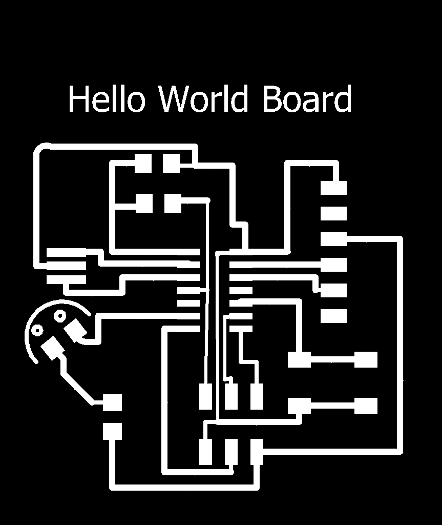
I downloaded the hello board .png.
My instructer and few other fello students adviced me to use AutoDesk Eagle as a PCB designing software.
I downloaded the sofware and installed it on my windows system. The procedure is fairly simple and one can dowwnload the free software from the official Auto desk website.
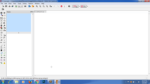
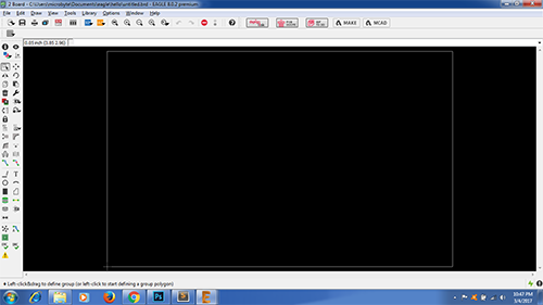
There are 2 stages in designing a PCB in Eagle
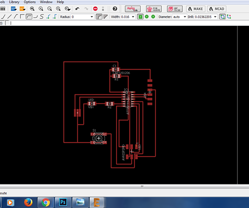
1- Designing a schematic in Schematic section- this consists of adding the components of our PCB, assigning values to the components and specifying the connections between them.
2-Design the track in the Board section - this is an important part as this will decide the route of connections of various components of the PCB.
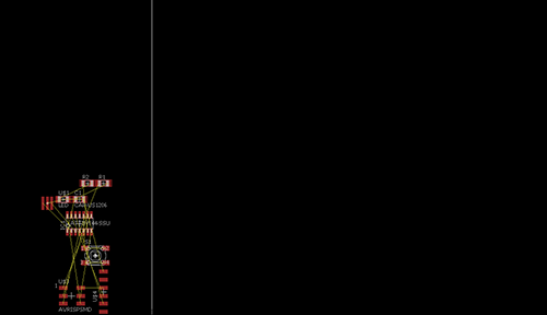
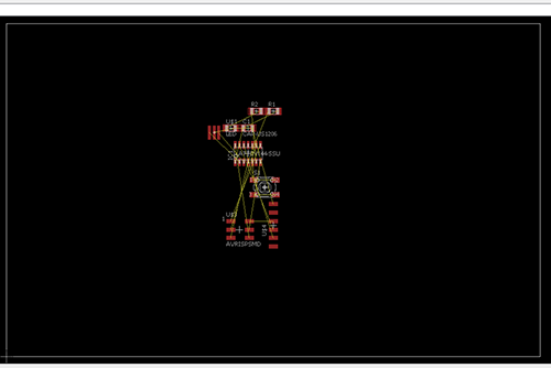
Schematic and Board sections of Eagle
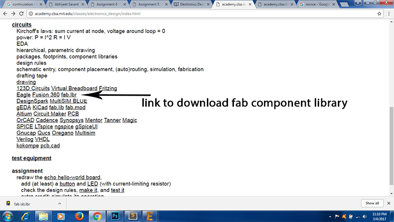
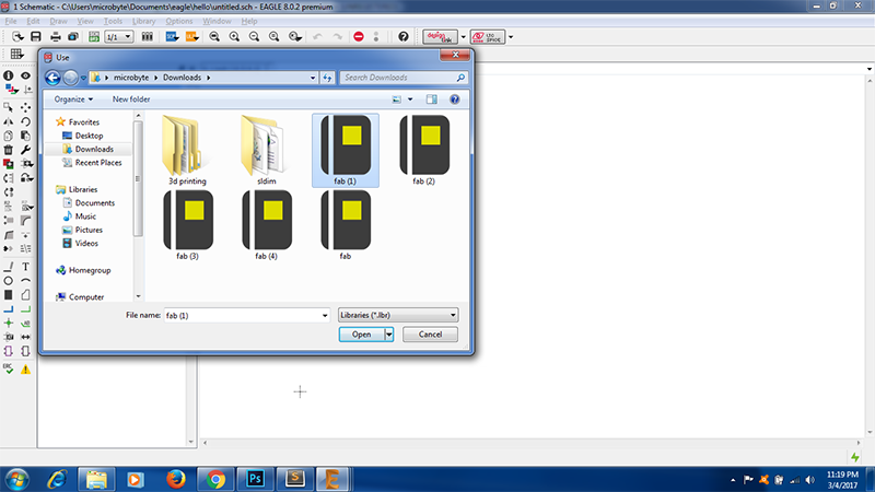
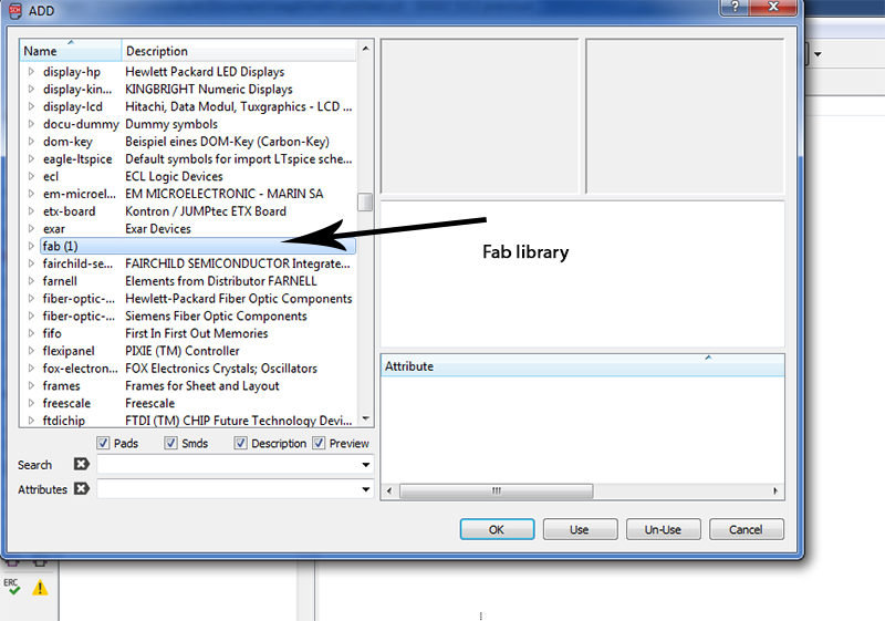
First step to download the Fab labs Component library and add it into your Eagle components library.
To do this type use in the command line of Eagle and search for the folder where you have downloaded the Fab Component library and open it.
To ensure that the library has been added, type add in the command line and find the fab library.
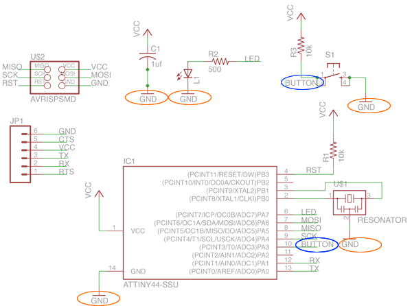
We start with shcematic, here add all the components you want in the PCb, in my case I added, capacitor, resistor, two connectors and Attiny 44.
As a modification in my circuit I decicded to add a LED with current limitting resistor and a switch
Now its just a question of connecting the components as per the drawing.
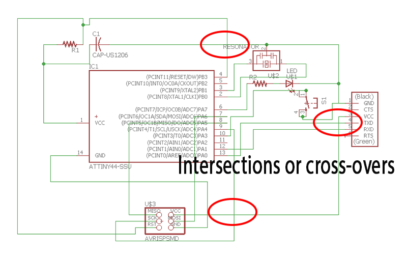
Remember, in schematic it is alright to intersect or cross- over the connections, Schematic is just spcifying the relation between the components.
I followed the tutorials given on Fab Academy website and joined the extra components as shown.
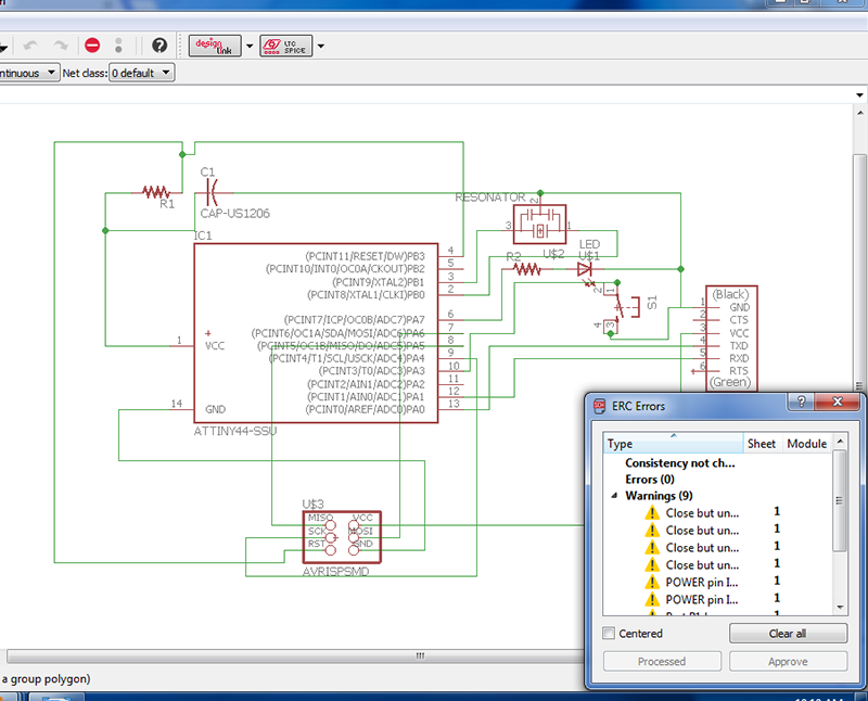
Before switchig to board we have to take an ERC, this is a check which will give us warnings and errors related to the elecrical connections.
If errors are found we have the options to repair or approve the errors, it is recommended to repair the errors in schematics.
Intersecting connectionsReference PCB design
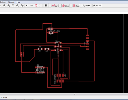
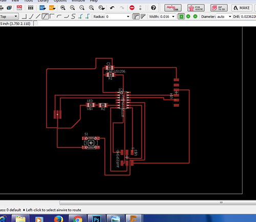
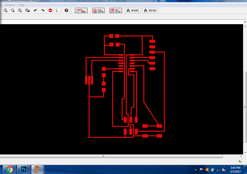
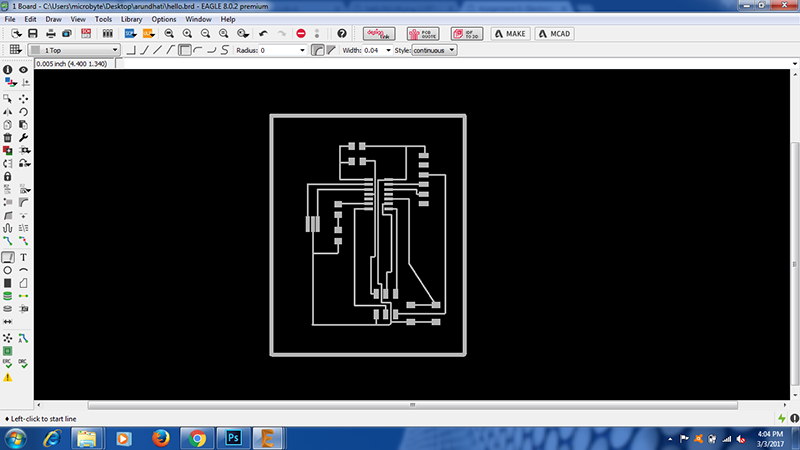
Now we we move switch to board in Eagle, the components will be placed outside the boundary which we have to drag into the box and start placing them in such a way that we can make paths between them without intersecting any other.
Switching to board
Now we route the track, for this right click the yellow lines and select route, this will bring a trace in red colour which we can direct as we want.
To assist the process there a lot of options, we can rotate, move, mirror the components. This helps us to orient the components in such a way that no two tracks cross each other.
Now its just a question of solving puzzle, connecting the dots and getting the track to as small as possible. We have to keep in mind the bed sze of our modella machine and the final use of the modella machine.
Making the PCB smaller in stages.
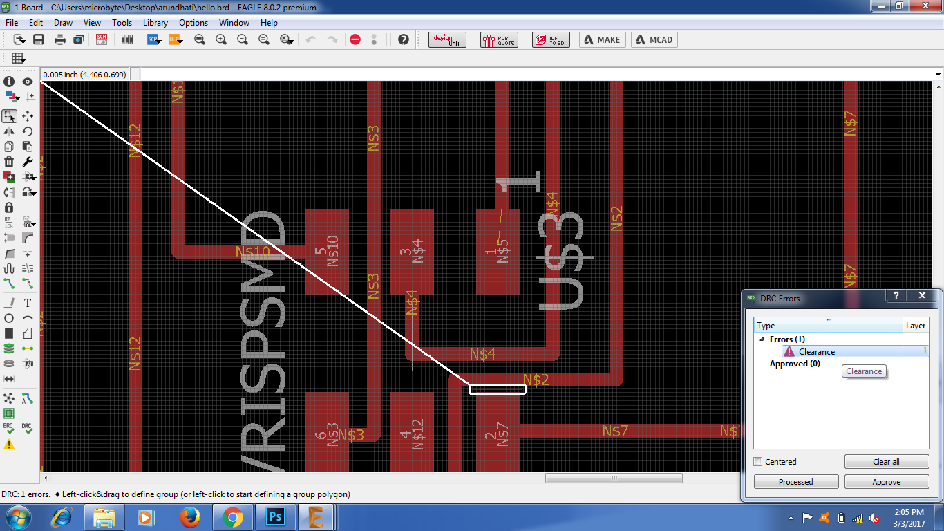
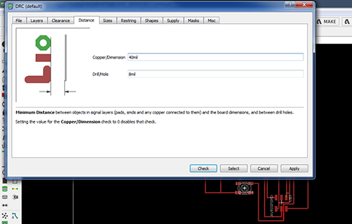
Now that the PCB is reduced to the size we want to take a DRC, This checks the dimensions and the clearance of our circuit. We have to rectify the errors given here as these generally are erros related to clearance of the tracks.
Typical erros found out by DRC
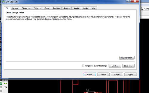
We can edit the values of the check, it is although recomended not to. We can set the values according to the resolution of our modella machine.
Adjusting the values of clearnace and dimensions
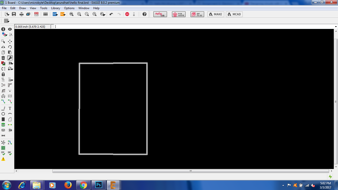
Now before moving to the modella machine, we have to set the boarder of the PCB along which the PCB will be cut in modella machine, For this we have to adjust the dimension layer according to the PCB size we want, adjust its thickness by typing change in the command boxand selecting widht.
We can also add text in the PCB. After adjusting the colour and thickness the final output should look like this
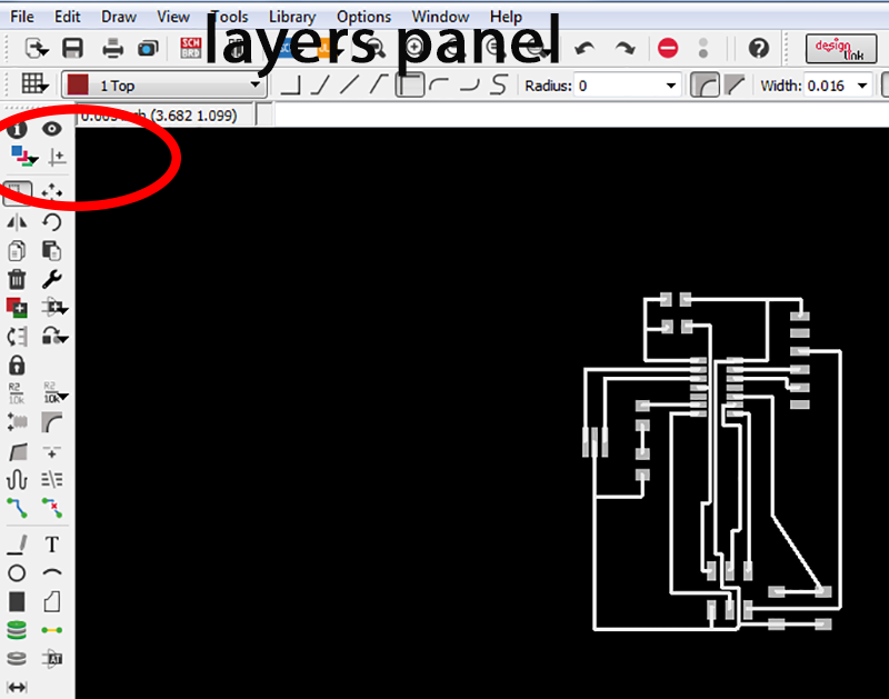
Now we have to save seperate .PNG file for traces and interior For this in layers panel, select top layer and deselect all the other layers, this will make only the traces visible.
Export this file as .PNG, this becomes the traces file.
For the interior file do the same except choose the layer dimensions and deselect every other layer and export the image as a.PNG
There is also an option to Auto Route which basically makes the tracks for us except for those which are not possible to make without intersection. The remaining tracks can be made manuaally as discribed above.
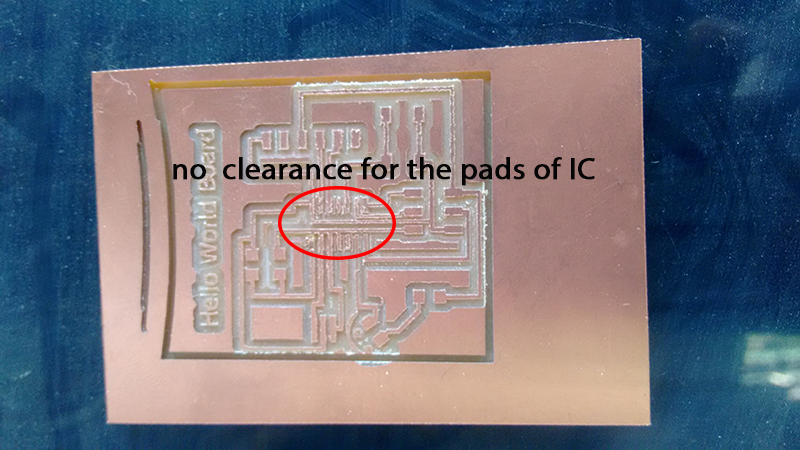
I realised that the first PCB I milled had a track thickness of 0.406mm which was very thin, thus I decided to change the thickness of the tracks. There was no clearance in the paddings of the IC This time I increased the width to 0.6096mm which seemed fine.
track width too small
To do this type change in the command box and select width and set it to 0.6096mm. This time the width of was fine after milling the PCB
Trouble shooting
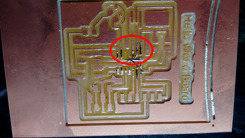
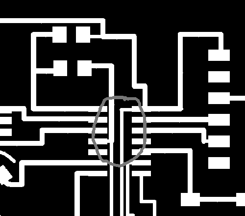
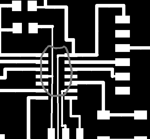
As the width of the track was increase I realised the track passing through the IC(ATTiny44) was touching the pads of the IC, this would result in total failure of the PCB, I tried to cut the track where it was touching the pads, but I failed to do so. The whole track was being ripped off from the board.
Thus I again went back to Eagle board and reduced the size of the tracks passing through the IC to 0.3089mm
Changing the width of the tracks passing through the middle of the IC
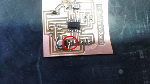
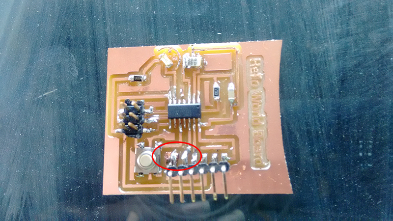
There was yet another problem, while soldering I accidentally ripped of the padding where the Six pin connector was going to connect. The copper layer came off and the track had no conducting material to attach to.
Fortunately this padding was not attached to any tracks.
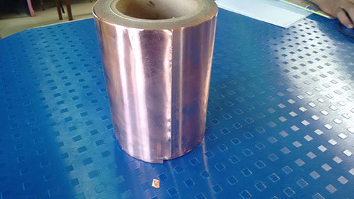
To correct this I used th copper foil and cut a piece approximately to the size of the padding and stuck it to the PCB by soldering it to the adjacent external part of the PCB.
Finally the problem was fixed, now the connecor sits nicely on the track. In India this is called as Juggad
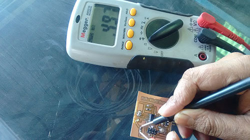
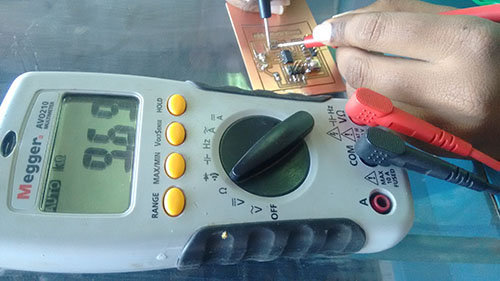
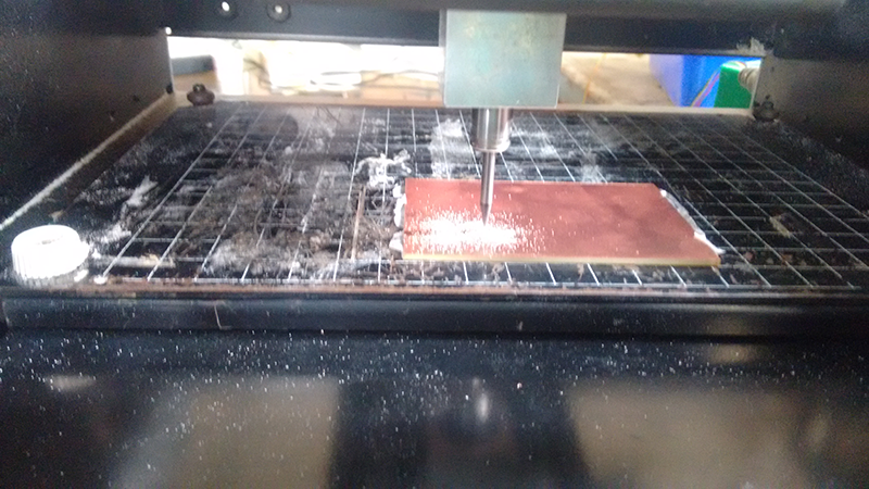
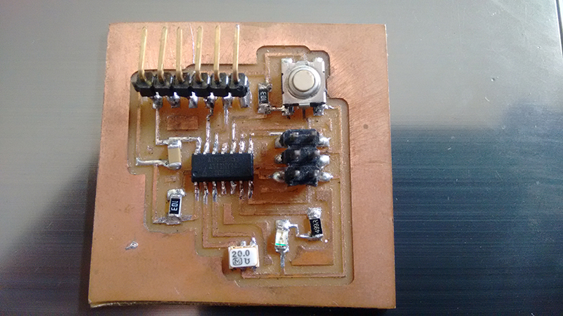
After everything was set I milled the PCB and soldered the components on it, I messed up the PCB in the last assignment thus I checked the continuity and resisitance value of the PCB with a multimeter.
After checking the continuity there were few loose connections detected which were corrected.
I figured out that the refurbished track is going to rip off some day as we use the board.
I stuck to Neil's policy of one board per week and made a new hello board
It is working, this board I used in the Embedded programming week